Capabilities
Our Fabless Manufacturing Model
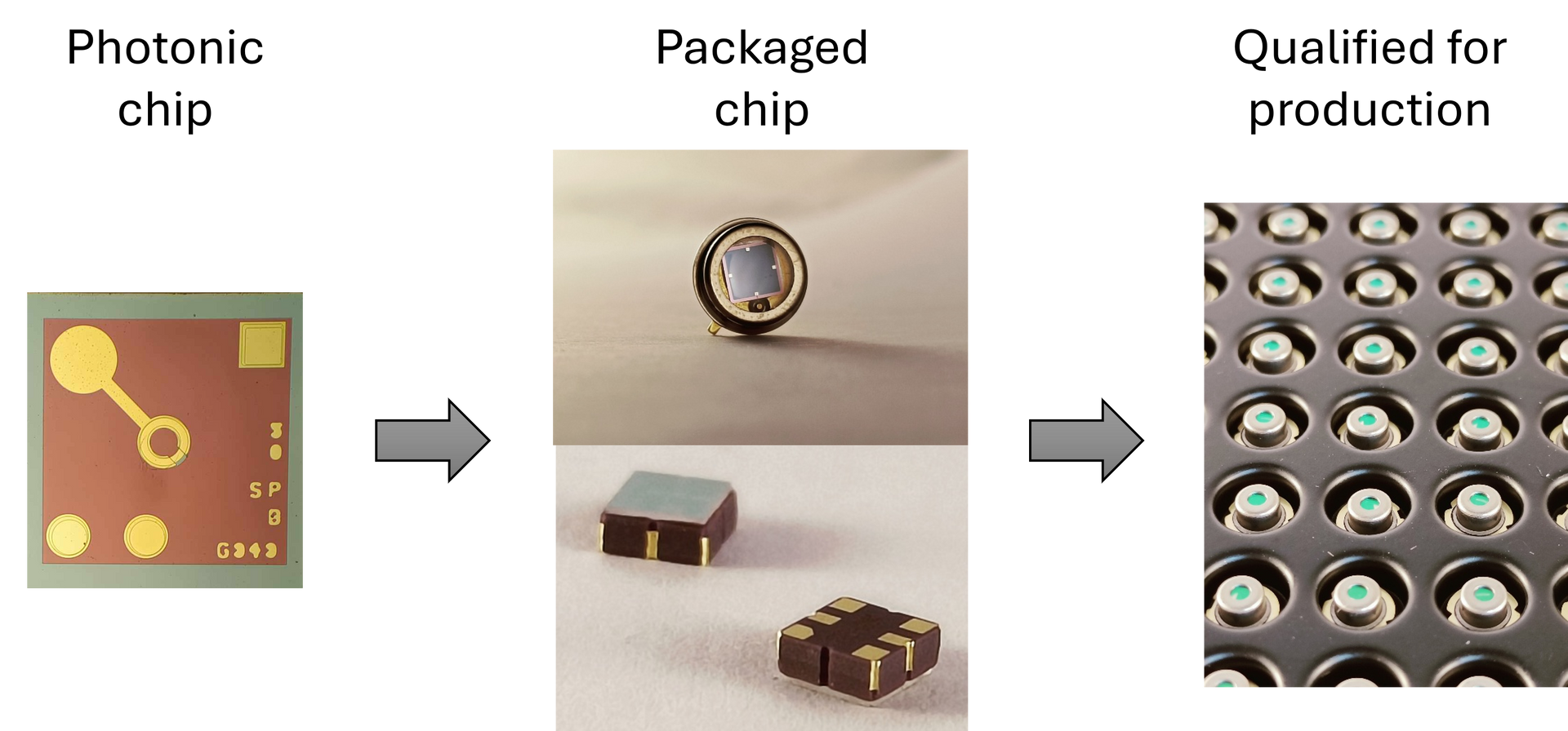
We operate a fabless approach, focusing on design, innovation, and product qualification while partnering with world-class foundries for wafer fabrication. This enables us to deliver high-performance photodetectors and laser diodes efficiently and cost-effectively.
The process illustrated below shows the key stages:
- Photonic chip – designed in-house or sourced from trusted foundries
- Packaged chip – assembled into reliable formats (TO, SMD, pigtail)
- Qualified for production - Rigorous quality control and testing
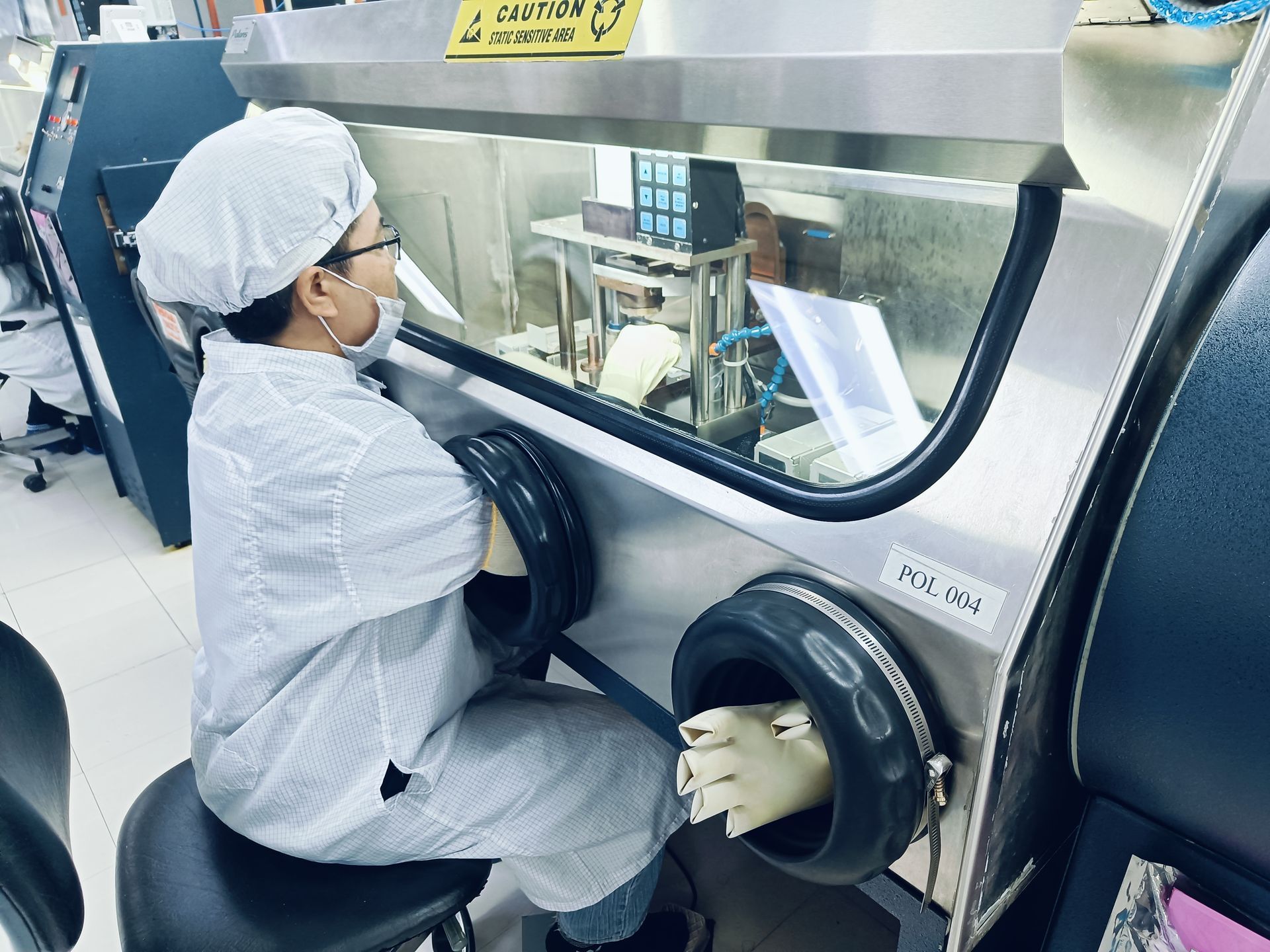
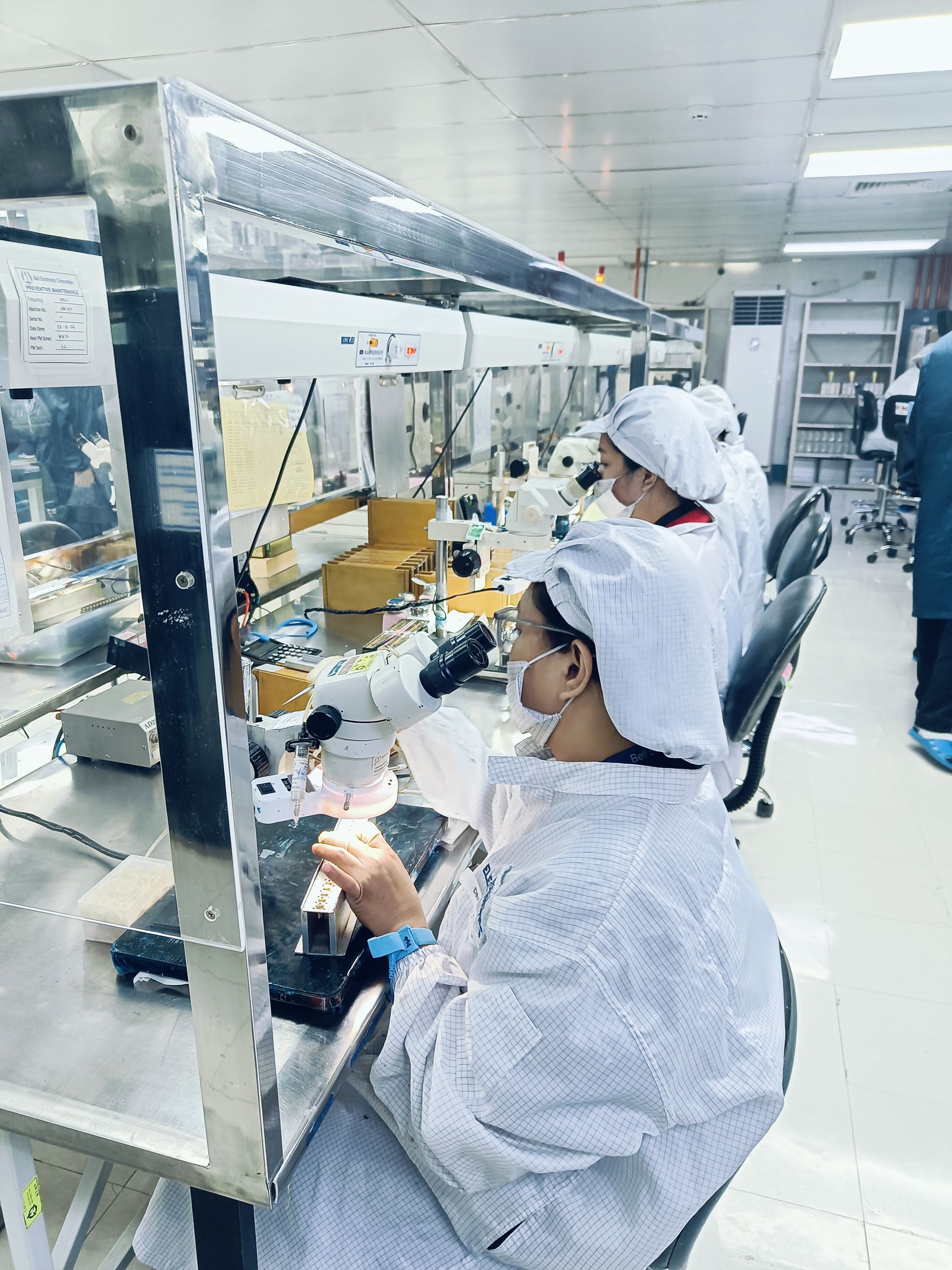
State-of-the-art packaging, testing and qualification off-shore facilities
We collaborate exclusively with reliable, trusted, and secure partners for assembly, testing, qualification, and foundry services. These long-term partnerships undergo rigorous vetting and auditing to ensure the highest standards of quality, confidentiality, IP protection, and supply chain security.
This approach allows us to deliver consistent, high-performance photonic solutions while providing our customers with peace of mind and dependable results.